Wednesday 26 September 2012

Light Sensor with Twilight Detection

This is not the first light sensitive circuit to be published in Elektor magazine. This circuit however, distinguishes itself that in addition to light and dark it can also signal twilight (dusk). This lets you automatically turn on a light in the living room when it becomes dark and turn on a lamp in a dark hallway when dusk sets in.


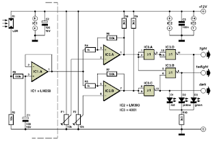
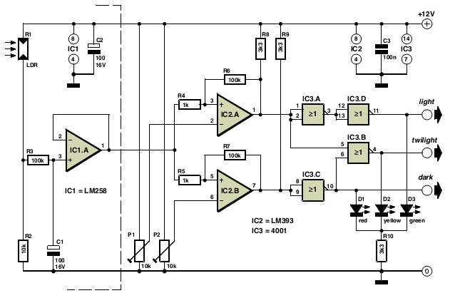
The circuit described here generates a logic signal on three separate out-puts for light, twilight and dark. The transition thresholds are set with two trimpots.The part of the circuit that is to the left of the dashed line can be located outside, on the roof, for example. This is possible because the LM258 can withstand frost, unlike the LM358, for instance. R1 and R2 together form a light dependent voltage divider, the voltage variations of which are damped by R3 and C1. This is desirable so that the circuit is less sensitive to birds that could cause the curtains to be closed when they fly across the sensor.
Opamp IC1a is wired as a buffer, so that the voltage that is seen by the remainder of the circuit does not deviate too much from the voltage ‘on the roof’. Any arbitrary LDR is suitable for R1, but do make sure that the voltage level at pin 3 of IC1a is at least 2 V below the power supply voltage when it is light. This is because that is the maximum voltage that IC1 and IC2 can tolerate at their inputs. Otherwise fit an additional resistor of, for example, 2.2 kΩ between R1 and the power supply. Two comparators (IC2a and IC2b) compare the incoming voltage with the threshold voltages set by P1 and P2. R4 and R6 (R5 and R7) prevent that that output of IC2a (IC2b) will jitter around the threshold. R8 and R9 have been added because IC2 has open-collector outputs.
It is actually already possible to determine whether it is light, dark or twilight by looking at the outputs of IC2a and IC2b, but the four gates of IC3 turn these into three separate signals. To make the adjustment easier, there are three LEDs of different colour connected to the outputs: green for light, yellow for twilight and red for dark. In the box is a description of the steps that are necessary to adjust the circuit.
It is best to do this towards the evening, that is when it is still light outside before the fall of dusk.To adjust the threshold values, P1 is intended for the transition from light to twilight and P2 for the transition from twilight to dark. With a correctly adjusted circuit, the voltage at the wiper of P1 has to be lower than the voltage at the wiper of P2.Because the outputs of the CMOS gates can-not drive heavy loads, low-current LEDs are essential. These have enough with only 2 mA, while ordinary LEDs will often need 20 mA. The power supply voltage can be from 9 VDC to 15 VDC.
Adjustment :
  1. First turn the wipers of both P1 and P2 to ground. If all is well only the green LED should be on.
  2. Wait until dusk falls.
  3. Now turn P1 just to the point where the green LED turns off and the yellow LED just turns on.
  4. Now wait until it is dark.
  5. Turn P2 just to the point where the yellow LED turns off and the red LED turns on. The adjustment is now complete.

Friday 21 September 2012

new website

hello frends
i create my new website please check it


http://ominfotechsystem.webnode.com

Tuesday 18 September 2012

gate syllabus for EC syudent

Linear Algebra: Matrix Algebra, Systems of linear equations, Eigen values and eigen vectors. 

Calculus: Mean value theorems, Theorems of integral calculus, Evaluation of definite and improper integrals, Partial Derivatives, Maxima and minima, Multiple integrals, Fourier series. Vector identities, Directional derivatives, Line, Surface and Volume integrals, Stokes, Gauss and Greens theorems. 

Differential equations: First order equation (linear and nonlinear), Higher order linear differential equations with constant coefficients, Method of variation of parameters, Cauchys and Eulers equations, Initial and boundary value problems, Partial Differential Equations and variable separable method. 

Complex variables: Analytic functions, Cauchys integral theorem and integral formula, Taylors and Laurent series, Residue theorem, solution integrals. 

Probability and Statistics: Sampling theorems, Conditional probability, Mean, median, mode and standard deviation, Random variables, Discrete and continuous distributions, Poisson, Normal and Binomial distribution, Correlation and regression analysis.

Numerical Methods: Solutions of non-linear algebraic equations, single and multi-step methods for differential equations. 

Transform Theory: Fourier transform, Laplace transform, Z-transform. 

ELECTRONICS AND COMMUNICATION ENGINEERING

Networks: Network graphs: matrices associated with graphs; incidence, fundamental cut set and fundamental circuit matrices. Solution methods: nodal and mesh analysis. Network theorems: superposition, Thevenin and Nortons maximum power transfer, Wye-Delta transformation. Steady state sinusoidal analysis using phasors. Linear constant coefficient differential equations; time domain analysis of simple RLC circuits, Solution of network equations using Laplace transform: frequency domain analysis of RLC circuits. 2-port network parameters: driving point and transfer functions. State equations for networks. 

Electronic Devices: Energy bands in silicon, intrinsic and extrinsic silicon. Carrier transport in silicon: diffusion current, drift current, mobility, and resistivity. Generation and recombination of carriers. p-n junction diode, Zener diode, tunnel diode, BJT, JFET, MOS capacitor, MOSFET, LED, p-I-n and avalanche photo diode, Basics of LASERs. Device technology: integrated circuits fabrication process, oxidation, diffusion, ion implantation, photolithography, n-tub, p-tub and twin-tub CMOS process.

Analog Circuits: Small Signal Equivalent circuits of diodes, BJTs, MOSFETs and analog CMOS. Simple diode circuits, clipping, clamping, rectifier. Biasing and bias stability of transistor and FET amplifiers. Amplifiers: single-and multi-stage, differential and operational, feedback, and power. Frequency response of amplifiers. Simple op-amp circuits. Filters. Sinusoidal oscillators; criterion for oscillation; single-transistor and op-amp configurations. Function generators and wave-shaping circuits, 555 Timers. Power supplies. 

Digital circuits: Boolean algebra, minimization of Boolean functions; logic gates; digital IC families (DTL, TTL, ECL, MOS, CMOS). Combinatorial circuits: arithmetic circuits, code converters, multiplexers, decoders, PROMs and PLAs. Sequential circuits: latches and flip-flops, counters and shift-registers. Sample and hold circuits, ADCs, DACs. Semiconductor memories. Microprocessor(8085): architecture, programming, memory and I/O interfacing. 

Signals and Systems: Definitions and properties of Laplace transform, continuous-time and discrete-time Fourier series, continuous-time and discrete-time Fourier Transform, DFT and FFT, z-transform. Sampling theorem. Linear Time-Invariant (LTI) Systems: definitions and properties; causality, stability, impulse response, convolution, poles and zeros, parallel and cascade structure, frequency response, group delay, phase delay. Signal transmission through LTI systems.

Control Systems: Basic control system components; block diagrammatic description, reduction of block diagrams. Open loop and closed loop (feedback) systems and stability analysis of these systems. Signal flow graphs and their use in determining transfer functions of systems; transient and steady state analysis of LTI control systems and frequency response. Tools and techniques for LTI control system analysis: root loci, Routh-Hurwitz criterion, Bode and Nyquist plots. Control system compensators: elements of lead and lag compensation, elements of Proportional-Integral-Derivative (PID) control. State variable representation and solution of state equation of LTI control systems. 

Communications: Random signals and noise: probability, random variables, probability density function, autocorrelation, power spectral density. Analog communication systems: amplitude and angle modulation and demodulation systems, spectral analysis of these operations, superheterodyne receivers; elements of hardware, realizations of analog communication systems; signal-to-noise ratio (SNR) calculations for amplitude modulation (AM) and frequency modulation (FM) for low noise conditions. Fundamentals of information theory and channel capacity theorem. Digital communication systems: pulse code modulation (PCM), differential pulse code modulation (DPCM), digital modulation schemes: amplitude, phase and frequency shift keying schemes (ASK, PSK, FSK), matched filter receivers, bandwidth consideration and probability of error calculations for these schemes. Basics of TDMA, FDMA and CDMA and GSM.

Electromagnetics: Elements of vector calculus: divergence and curl; Gauss and Stokes theorems, Maxwells equations: differential and integral forms. Wave equation, Poynting vector. Plane waves: propagation through various media; reflection and refraction; phase and group velocity; skin depth. Transmission lines: characteristic impedance; impedance transformation; Smith chart; impedance matching; S parameters, pulse excitation. Waveguides: modes in rectangular waveguides; boundary conditions; cut-off frequencies; dispersion relations. Basics of propagation in dielectric waveguide and optical fibers. Basics of Antennas: Dipole antennas; radiation pattern; antenna gain.

i says....

if you like my blog than make follower of the blog and follow the blog.....


thank you

regard

Raj Trivedi
trivedi.raj8@gmail.com
9662010710

Analog-to-digital converter (ADC ) Interfacing with microcontroller


This post is the continuetion of last post in which we discussed the Analog interfacing with microcontroller. We learnt that the transducers required --- in middle to have interfacing with microcontrollers. This post is about the ADC interfacing and working.
Thus we can say that we need to have some means to convert the analog signal of transducers into digital signal so that computers can handle it and further processing could be done.
Analog-to-digital converter (ADC) is a device which can convert analogue voltage to digital numbers so that microcontrollers can handle and process the data. This is required to obtain some meaningful results or any useful work with micro controller. ADCs are the most widely used devices for data acquisition and control. Some microcontrollers have built in ADCs but the 8051 micro controller don't have any built in ADC. So we have to use external ADC for said purpose. There some common and important features about ADCs. for example, resolution of adc, response time of adc , mode of workand method of conversion. ADC has n-bit resolution, where n can be 8, 12, 16 or even 24 bits. The higher-resolution ADC provides a smaller step size.Step size is the smallest change that can be recognized by ADC. The heart of any current computational device relies upon digital bits, voltage states which can be at either high or low voltages. One of the simplest constructions, the ADC, converts an analog voltage signal to a digital one. Analog to Digital converters, and their counterparts,Digital to Analog converters are used all the time in electronics. Indeed, they provide the only method by which one may interface a digital system with the real world, which functions in analog.Digital data acquisition and conversion systems are ubiquitous, being found in virtually every modern communication, digital signal processing (DSP), electronic instrument, and micro-controller applications. Regardless of the sophistication of the application, a data acquisition and/or conversion system will consist of some pre-processing elements, a domain conversion device (digital to analog conversion (ADC) or analog to digital conversion (DAC)), controller, and post-processing agent. 

8-Bit resolution ADCs:-

An ADC has a resolution of 8 bits, the range is divided into 2^8=256 steps (from 0 – 255). But there are 255 quantization levels.
how step size of ADC is calculated equation for step size

Where the Vcc is the reference voltage of ADC with n-bit resolution.Below is table in which Resolution versus Step Size for ADC (if Vcc = 5V) is provided.
Resolution versus Step Size for ADC
ADC0804 Chip (Free Running Mode)
There are some control PINs and some input and other are output PINS of ADC0804. The pin configuration of ADC0804 is shown in the figure below.
ADC0804 Chip Free Running Mode
Important pins are discussed here in some detail.
CS  :Active low input used to activate the ADC0804 chip.

RD (data enable)  : Active low input used to get converted data out of the ADC0804 chip. When CS = 0, if a high-to-low pulse is applied to the RD pin, the 8-bit digital output shows up at the D0-D7 data pins.

WR (start conversion): Active low input used to inform the ADC0804 to start the conversion process. If CS = 0 when WR makes a low-to-high transition, the ADC0804 starts converting the analog input value of Vin to an 8-bit digital number. When the data conversion is complete, the INTR pin is forced low by the ADC0804.
CLK IN and CLK R : Connect to external capacitor and resistor for self-clocking, f = 1/(1.1RC). The clock affect the conversion time and this time cannot be faster than 110 micros.

INTR (end of conversion) This is an active low output pin. When the conversion is finished, it goes low to signal the CPU that the converted data is ready to be picked up. After INTR goes low, we make CS = 0 and send a high-to-low pulse to the RD pin to get the data out of the ADC0804 chip.
ADC0804 Chip step size calculation


Vin (+) and Vin (-) :These are the differential analog inputs where Vin = Vin (+) - Vin (-). Often the Vin (-) pin is connected to ground and the Vin (+) pin is used as the analog input to be converted to digital.
VCC : This is the +5V power supply. It is also used as a reference voltage when the Vref/2 (pin 9) input is open.
ADC0804 Chip step size calculation ADC0804 has resolution of 8 bits
Pin Vref/2 is open, Step size =19.6mV

Vref/2 :- Input voltage pin used for the reference voltage. If this pin is open, the analog input voltage for the the ADC is ranged from 0 to 5 volts.This is optional input pin. It is used only when the input signal range is small. When pin 9 is at 2V, the range is 0-4V, i.e. Twice the voltage at pin 9. Pin 6 (V+), Pin 7(V-): The actual input is the difference in voltages applied to these pins. The analogue input can range from 0 to 5V.

D0 – D7 output PINs of ADC: D0 – D7 are the digital data output pins. These are the tri-state buffered and the converted data is accessed only when CS = 0 and RD is forced low. The output voltage:


Analog Ground and Digital Ground :- Analog ground is connected to the ground of the analog signal while digital ground is connected to the ground of the Vcc pin.
Operation of the ADC
The analog signal should be connected to Vin.
To start conversion: WR should be pulled low and RD should be high.
When the conversion is complete, the ADC0804 will pull INT low.
To make the binary result available at the outputs of the ADC, RD should be low.

Tags:-
Digital Audio Compression Storage and Retrieval System (DACSRS),‑The ADC0804 is a successive approximation type A/D converter ,connection of temperature sensor with ADC0804 ,Automated Object Avoiding Robot Project,Transducer coverts physical variable to an electrical signal ,Design and implementation of frequency converter and signal recovery circuits. ,ADC0804 IC is a CMOS 8-bit A/D converter featuring fast conversion times,DATA CONVERSION,LEVEL & TEMPERATURE CONTROLLER, How to build a digital oscilloscope based on the ADC0804 Flashy acquisition board The interfacing of LM35 Temperature Sensor using ADC0804.

Monday 17 September 2012

PWM with microcontroller 8051 for SCR or triac power control


The project "PWM with microcontroller 8051 for SCR or triac power control" can be used for two applications.
1. To control AC load's power with SCR or triac by controlling the firing angle or duty cycle for two channels.
2. The project as it is can be used as digital to analog converter "DAC" for two channels.

This project is currently output two PWM signals but can be extended to many PWM signals very easy. The input to the microcontroller is 100HZ pulses as zero crossing.

The project can be used to control the heating of AC heater also.
currently it is build for two channel DAC, the input at port1 and port2 of microcontroller is converted to 0 - 5v accordingly. But if it is desired to control the SCR, then OP-AMP circuit will be removed and optocoupler moc3020 will be used for interfacing SCR or triac.

The circuit diagram of PWM with microcontroller 8051 for SCR or triac power control is as under:


The code of program for PWM with microcontroller 8051 for SCR or triac power control is written c lanuage using keil compiler. The c-code for PWM is as follows.
/* This project is develop to generate two seperate channel PWM signals at 50HZ frequency
The duty cycle of the pulses is variable subject to the input on Port1 and port2.
The output PWM signal can be used to drive SCR or triacs to control the phase angle and power of any load with suitable hardware interface.
Please not that in this project the OPAMP are used to convert the pulses to 0 - 5 V, means you can use it in as two channel DAC also.
But for triac or SCR interface the OPAMP circuit will be re-placed with proper optocoupler like moc3020 and scrs.89c51 as pwm controller
*/

#include<at89x52.h>
unsigned char ch_count[2];// two channel counts array
unsigned char ch_duty_level[2];// level of the duty cycle
bit int_10ms;// this is a flag wich is set every 10msec time period
sbit PWM1 = P3^6;
sbit PWM2 = P3^7;
sbit indicator = P3^5;
void external_interrupt (void) interrupt 0
// external interrupt for zero crossing dectection
{
ch_count[0]=ch_duty_level[0];
// on zero crossing detection, counts are updated for both PWM channels
ch_count[1]=ch_duty_level[1];
PWM1=0; // the output is active low
PWM2 =0;//89c51 as pwm controller
int_10ms = 1; // 10msec flag is set
}
void timer_interrupt (void) interrupt 1
// The timer 0 is used for the duty cycle adjustement of two channel PWM
{
TL0 = 0XE2; //reset timer LSB

if(--ch_count[0]==0) PWM1 = 1;
// each time the timer interrupt occur the counts are decreased by one and on reaching zero
if(--ch_count[1]==0) PWM2 = 1;
// the outputs are turned off, as the out put is active low

}
void main (void)
{

ET0 = 1; // enables the Timer 0 interrupt of 8051
TMOD = 0x02;
// timer mode register, timer 0 is used in mode 2
TL0 = 0XE2; // Initialize timer0 LSB
TR0 = 1; // timer 0 is activated
EX0 = 1; // external inturpt is activated
IT0 = 1;
EA = 1;
ch_duty_level[0] = 30; // dummy value for duty cycle for PWM 1
ch_duty_level[1] = 60; // dummy value for duty cycle for PWM 2
while (1) // endless loop
{
if( int_10ms){
int_10ms = 0;
ch_duty_level[0] = P1;
// take the input value of duty cycle for PWM 1 fromport1 of the 8051
ch_duty_level[1] = P2;
// take the input value of duty cycle for PWM 2 fromport1 of the 8051
indicator =~ indicator;
}
}
}


solenoid valve atmel dc control triac,dimmer bt138,uln2003 microcontroleur interfacing a microprocessor to a power thyristor microcontrol based level mesurement 89c51 as pwm controller,at89c2051 sine wave pwm

Tuesday 11 September 2012

PS2 keyboard interface with micro controller

hello frends

here i teach you how to interface PS2 keyboard interface with micro controller


first you have to understand the basic concept of PS2 pin for that here i attach one PDF file related to it...

link is :-

http://students.iitk.ac.in/eclub/assets/tutorials/PS2Keyboard.pdf